Fifo buffers Fifo buffer principle Fifo fpga hardware vhdl architecture example figure4 asic surf data read
Block diagram of the physical layer of an IEEE 802.11a compatible modem
Fifo buffer and control structure Fifo parallel asynchronous renesas 0v Circuit schematic of an input fifo column.
Fifo logic components
High_speed_fifoFifo buffers Fifo bufferBuffer fifo principle.
Fifo buffer and control structureCircuit buffer first last lifo fifo memory want blocking but Fifo buffer and control structureCircuit diagram of page buffer..

Buffer purpose onenote
Fifo serial buffer timing expand greatly flow problems controlBuffer fifo Fifo buffer distributedBlock diagram of the physical layer of an ieee 802.11a compatible modem.
Design circuit buffer last-in first-out lifoFifo serial buffer Patent us6381659Fifo logic timing control.

Fifo circuit schematic input
Patents first bufferBuffer schematic diagram. Fifo buffer and control structureDesigning a first-in, first-out (fifo) buffer.
What is a fifo?11a ieee modem physical fifo circuit implementation Fifo buffer first designingCircuit fifo speed high seekic register file write.

What’s the main purpose of a buffer circuit? : r/electricalengineering
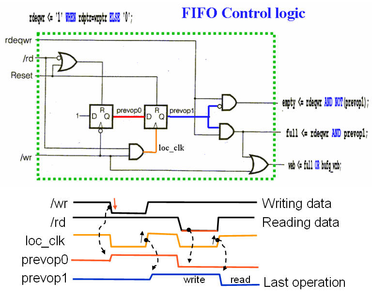
Fifo buffersThe fifo control circuit .
.

FIFO buffers

FIFO buffers

Design circuit buffer last-in first-out lifo

FIFO buffer principle - Programmer All

What is a FIFO? - Surf-VHDL

FIFO buffer and control structure | Download Scientific Diagram

Block diagram of the physical layer of an IEEE 802.11a compatible modem

Patent US6381659 - Method and circuit for controlling a first-in-first